HIGH QUALITY RECORDING OF BIOELECTRIC EVENTS. II : A LOW-NOISE,
LOW-POWER MULTICHANNEL AMPLIFIER DESIGN
A. C. Metting van Rijn, A. Peper, C. A. Grimbergen
Laboratory of Medical Physics, University of Amsterdam, Academic
Medical Center, Meibergdreef 15, 1105 AZ Amsterdam, The Netherlands
- Keywords - Bioelectric recordings, multichannel front end, low-noise, low
power consumption, small dimensions.
- Abstract - A multichannel instrumentation amplifier, developed to be used in
a miniature universal eight channel amplifier module, is described. After discussing the
specific properties of a bioelectric recording, the difficulties of meeting the demanded
specifications with a design based on operational amplifiers are reviewed. Because it
proved impossible to achieve the demanded combination of low noise and low power
consumption using commercially available operational amplifiers, an amplifier equipped
with an input-stage with discrete transistors was developed. A new design concept was used
to expand the design to a multichannel version with an equivalent input noise voltage of
0.35 micro;Vrms in a bandwidth of 0.1 - 100 Hz and a power consumption of 0.6 mW per
channel.
The results of this study are applied to miniature, universal, 8 channel amplifier
modules, manufactured with thick-film production techniques. The modules can be coupled to
satisfy the demand for a multiple of 8 channels. The low power consumption enables the
modules to be used in all kinds of portable and telemetry measurement systems and
simplifies the power supply in stationary measurement systems.
1. INTRODUCTION
In present biomedical research, recording systems with a high number of measuring
channels are often required. Examples of multichannel recordings are brain mapping: EEG
measurements with 20 channels (Duffy, 1982), 28 channels (Gruzelier et al., 1988) or 36
channels (Duff, 1980) and body surface mapping: ECG measurements with 64 channels (Reek et
al., 1984; Spekhorst et al., 1990). Over the last years, large progress has been made in
the development of the digital part of recording systems with respect to the processing of
the large amount of data gathered. The quality of the analog front end, however, has
remained much the same and in many cases does not stand up to its task. The proper
measurement and amplification of bioelectric signals present some specific problems.
General amplifier design techniques are well developed and extensively described in
literature. However, in designing a biomedical amplifier much attention should be paid to
the special character of a bioelectric measurement. The fact that electrodes are used as
signal transducers in bioelectric recordings has important consequences for the required
performance of the amplifier. Because of its impedance, offset voltage and noise
contribution, the electrode-skin interface may cause various problems, especially in
multichannel recordings. Finally, the goal to make the amplifier applicable to many
different bioelectric (multichannel) measurement situations received extra consideration.
2. AMPLIFIER DESIGN CRITERIA
The electrode-skin interface has a complex impedance between 1 k and 1 M at 50 Hz
(Almasi and Schmitt, 1970; Grimnes, 1983; Geddes, 1972; Rosell et al., 1988). The
electrode-skin impedance depends on many factors like skin condition and preparation, and
large variations in electrode-skin impedance can be found. High electrode-skin impedances
and/or large differences between the electrode-skin impedances may cause the measurement
system to be susceptible to several forms of interference. The theory was extensively
treated in a previous study (Metting van Rijn et al., in press). To ensure correct
operation with typical electrode-skin impedances and typical interference sources, an
amplifier should meet the following demands:
- very high common mode input impedance (> 100 M at 50 Hz, )
- high differential mode input impedance (> 10 M at 50 Hz, )
- equal common mode input impedances for all inputs
- high common mode rejection ratio (> 80 dB at 50 Hz)
- shielded input cables, the shields must be driven by a proper guarding circuit
(Morrison, 1977; Metting van Rijn et al., in press)
- additional reduction of common mode voltage with a driven right leg circuit (Winter and
Webster, 1983; Metting van Rijn et al., in press)
The electrode-skin interface forms a galvanic half-cell (Geddes, 1972). The exact
half-cell voltage of a electrode-skin interface depends mainly on the condition of the
skin and electrodes. To the signal measured between the electrodes, the difference between
the half-cell voltages of the electrode-skin interfaces must be added. This voltage
usually varies slowly during a recording, resulting in a low frequent noise signal. An
amplifier should suppress these relatively large (several tens of millivolts),
low-frequency input signals in order to prevent saturation. A cut-off frequency of
approximately 0.15 Hz for the high-pass filtering is commonly used for this objective. The
signal magnitude that minimally can be measured is defined in principle by the thermal
noise of the electrode-skin impedance (Et = 1.3 x 10⁻³ Re micro;Vrms in a
bandwidth of 0.1 - 100 Hz). In practice however, noise levels this low are almost never
obtained due to variations in the half-cell voltage of the electrode-skin interface. In
order to be able to decide about clinical death, an equivalent input noise level lower
than 2 micro;Vp-p in a bandwidth of 0.1 - 30 Hz is mandatory for clinical EEG amplifiers
(Cooper et al., 1969; Silverman et al. 1969). Consequently, the target value for the
equivalent input noise voltage in this study is chosen to be 0.5 micro;Vrms in a bandwidth
0.1 - 100 Hz . An equivalent input noise current less than 5 pArms in a bandwidth of 0.1 -
100 Hz is demanded to ensure that only a small amount of noise is added with typical
electrode-skin impedances (total equivalent input noise voltage is 0.6 micro;Vrms in a
bandwidth of 0.1 - 100 Hz with electrode-skin impedances of 50 k ).
In many multichannel recordings the signal differences between each of the measuring
electrodes and a common reference voltage is measured (monopolar recording). This
reference voltage is sometimes derived from one electrode but often the average voltage
from two (EEG) or three electrodes (ECG) is used (Clark, 1978; Geddes and Baker, 1975).
These measuring configurations should be considered when designing a multichannel
amplifier. Small dimensions are important for several reasons. It is obvious that small
dimensions will enable the amplifier module to be used in all kinds of portable and
telemetry measurements but a small size of the amplifier also reduces the capacitance
between the amplifier and its environment in an isolated amplifier set-up. Reduction of
this capacitance lowers the common mode voltage, which voltage is one of the main causes
for interference (Metting van Rijn et al., in press).
Minimum power consumption is important because it allows small sized batteries to be used
as power supply. This is of course essential if the amplifier module is used in ambulant
recordings but can present some important advantages in stationary measurement systems as
well. In a system which is powered by the mains supply by the use of an isolation
transformer, most of the capacitance across the isolation barrier is usually caused by the
power supply (Metting van Rijn et al., in press). A small battery-powered amplifier can be
designed to have very small capacitance to the environment, resulting in a low common mode
voltage. Another advantage is the greatly improved safety because there are no high
voltages present in the amplifier cabinet. Finally, batteries deliver a very
"clean" supply voltage which is essential for low-noise operation (Motchenbacher
and Fitchen, 1972). Mains supply voltages are often polluted with a lot of high-frequency
interference (spikes).
3. Biomedical amplifiers with operational amplifiers
Before concentrating on multichannel amplifiers it is instructive to review the almost
universally used instrumentation amplifier with three operational amplifiers, pictured in
Fig. 1A (Tobey et al.,1971). The advantages of the circuit are:
- Amplification of differential mode signals in the first stage (gain of 20 dB or more)
which makes the noise contributions from succeeding amplifier stages insignificant
(Motchenbacher and Fitchen, 1972).
- No amplification of common mode signals in the first amplifier stage. This feature makes
it possible to handle common mode voltages nearly as high as the supply voltage and to
achieve a high common mode rejection ratio without the need for precise resistor trimming
(Wong and Ott, 1976).
- A high and equal common mode input impedance for both inputs. This is an important
property as differences in electrode-skin impedance and/or common mode input impedances
convert common mode voltage into a differential mode voltage; this phenomenon is known as
the "potential divider effect" (Pacela, 1967; Huhta and Webster, 1973).

Fig. 1 : (a) Instrumentation amplifier with three operational amplifiers.
Biomedical amplifiers are usually based upon this design. The voltage at point Pav is
equal to the common mode voltage. (b) Multichannel instrumentation amplifier with
operational amplifiers. The circuit is an extension of the three operational amplifier
circuit of Fig. 1A and its favorable properties are preserved.
The three operational amplifier circuit, being widely available as a single monolithic
or hybrid IC, is an attractive choice as a building block for a multichannel amplifier
(Smit et al., 1987) when it is used as an independent instrumentation amplifier with its
own pair of measuring electrodes (bipolar recording). However, when the potential
difference between a number of electrodes and a common reference electrode is to be
measured (monopolar recording, for example clinical ECG and EEG measurements) the three
operational amplifier circuit is not optimal. It is tempting to interconnect several
amplifier inputs to obtain a common reference input. However, this method introduces
differences in common mode input impedance between the reference input and the other (not
interconnected) inputs resulting in an increase of interference due to the "potential
divider effect" (Metting van Rijn et al., in press). The inclusion of a buffer
amplifier at the reference input may prevent the degradation of common mode input
impedance but will add extra noise to the input signals, which are not amplified at this
point. A multichannel amplifier set-up without these drawbacks is shown in Fig. 1B. It is
basically an extension of the three operational amplifier configuration and all the
favorable characteristics mentioned above are preserved (O'Brien et al., 1983). Each input
signal is amplified with respect to the voltage at point Pav, which voltage is equal to
the average of the input voltages (= common mode voltage). Note that all amplifier inputs
are equal. For practical biomedical use the circuit is completed with appropriate
high-pass and low-pass filtering, guarding circuits and a driven right leg circuit. 4.
Biomedical amplifiers with discrete input stages In the present study, the goal was to
develop a miniature multichannel analog front end with optimal noise properties and
minimum power consumption. The specifications were based on the considerations given in
Section 2 and are listed in the first column of Table 1. The design had to be suitable to
be manufactured with thick-film production techniques which offers higher reliability and
far smaller dimensions than printed circuit board production techniques (Sergent, 1981).
Table I: Amplifier module specifications.
| Parameter |
Target |
Design
Fig. 3� |
| Equivalent input
noise voltage (�Vrms, 0.1 - 100 Hz) |
<
0.5 |
0.35 |
| Equivalent input
noise current (pArms, 0.1 - 100 Hz) |
<
5 |
4 |
| Bandwidth +0,-3 dB
(Hz) |
0.16-100 |
0.16-100 |
| Differential mode DC
input range (mV) |
>
150 |
190 |
| Differential mode AC
input range (mVp-p) |
>
20 |
25 |
| Common mode input
range (Vp-p) |
>
2 |
2.5 |
| Input bias current
(nA per input) |
<
50 |
23
+/- 5 |
| Gain: 500 500 -
differential mode input impedance (Mohm at 50 Hz) |
>
10 |
>
15 |
| Common mode input
impedance : with unshielded input leads (Mohm at 50 Hz) |
>
100 |
250 |
| Common mode input
impedance : with guarded input leads (M ohm at 50 Hz) (cable capacitance is 330 pF) |
>
100 |
200 |
| Common Mode
Rejection Ratio (dB at 50 Hz) |
>
80 |
91
+/- 5 |
| power consumption
(mW per channel) |
<
1 |
0.6 |
The amplifier design shown in Fig. 1B seemed attractive because of its simplicity.
However, with this circuit it proved impossible to achieve the desired combination of low
noise and low power consumption. It can be calculated (see Appendix A1 and A2) that it is
possible in theory to surpass our specifications (Table 1) with a power consumption 10 -
100 times lower than offered by currently available low-noise operational amplifiers. The
relatively high power consumption of operational amplifiers is mainly due to an extended
bandwidth which however is superfluous for most physiological applications. When
programmable operational amplifiers are used, they can be adjusted for a small bandwidth
and low power consumption but none of these devices has an acceptable noise level .
Therefore a multichannel instrumentation amplifier with a discrete input stage was
developed. An input stage based on discrete components can offer some important
advantages: the best discrete transistors are superior to the input transistors in IC
operational amplifiers (Nelson, 1980) and the increased design freedom allows the input
stage to be optimized for biomedical applications. In the next section a one-channel
version of the amplifier is described. In addition, a new concept for expanding a one
channel instrumentation amplifier to more channels was developed. The resulting
multichannel design that was used in the thick-film modules is described in section 6.
5. ONE-CHANNEL INSTRUMENTATION AMPLIFIER FOR BIOELECTRIC RECORDINGS
There was already experience gathered with a previously developed one-channel
instrumentation amplifier (Hamstra et al., 1984), Starting from that design an amplifier
which met more severe specifications was developed. The circuit is shown in Fig. 2 :
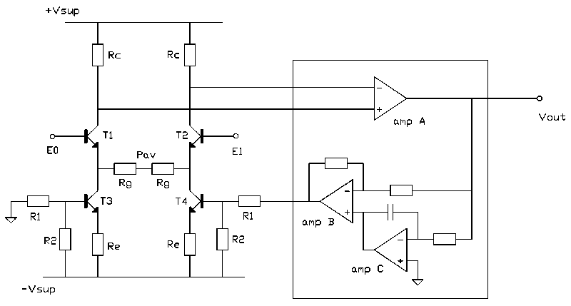
Fig. 2 : Simplified schematic of an instrumentation amplifier for biomedical
applications. The combination of low-noise and very low power consumption is achieved by
the use of discrete transistors in the input stage.
The input stage is based on the well known current balance amplifier circuit (Wong and
Ott, 1976; Graeme, 1977) with current sources T3 and T4 replacing the common emitter
resistor of the input transistors. The high output conductance of these current sources
provides a very high common mode input impedance . The bias of T3 is fixed, T4 is part of
the feedback circuit. In the second stage operational amplifiers are used to keep the
number of parts low. The programmable operational amplifiers used (LM4250, National
Semiconductor) can be set for very low power consumption while their rather high noise is
not troublesome because of the amplification in the first amplifier stage. Operational
amplifier "amp A" produces a single ended output. Operational amplifiers
"amp B" and "amp C" regulate the feedback signal. The design employs
the "current feedback" technique which offers high common mode rejection ratio,
without the need for very precise resistor matching. Operational amplifier "amp
C" is used as an integrator to provide maximum feedback for DC input voltages. DC
suppression without the need for large capacitors is accomplished with this circuit
(capacitors larger than 100 nF are difficult to apply with thick-film production
techniques).
The measured performance characteristics of the design of Fig. 2 are listed in Table 1,
second column. When high quality resistors (with a low excess-noise level, see Appendix
A2) are used, the equivalent input noise voltage is determined by shot-noise currents of
the four transistors in the input stage only. With the use of high quality transistors
(LM194, National Semiconductor) a compromise between low noise, low power consumption, DC
input range and differential mode input impedance was obtained superior to an input stage
made with operational amplifiers. A detailed description of how to find the best balance
between the various specifications is given in Appendix A1.
6. MULTICHANNEL INSTRUMENTATION AMPLIFIER FOR BIOELECTRIC RECORDINGS
When the circuit described in Section 5 is to be used in a multichannel amplifier for
monopolar recordings it is again not advisable to interconnect the inputs of a number of
independent instrumentation amplifiers. The situation is comparable with the one in
Section 3; the amplifier circuit itself must be adapted for multichannel use. We developed
an unconventional method to expand the design to more channels. In our multichannel
version, none of the good specifications of the one channel design is compromised. The way
the extension to more channels was accomplished is shown for n=2 in Fig. 3 (n = number of
channels).
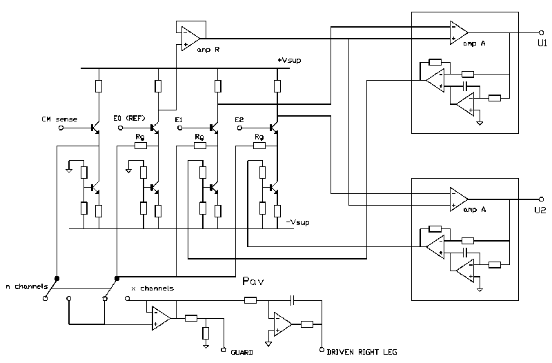
Fig. 3 : Simplified schematic of a multichannel instrumentation
amplifier with discrete transistors in the input stage. The circuit is based on the
one-channel design of Fig. 2. The amplifier is equipped with Guarding and Driven Right Leg
circuits and an additional CM-sense input stage.
The operation of the circuit is easily understood when the behavior of the circuit is
examined with the same (common mode) signal applied to all inputs. In this case the (AC)
currents in all sections are equal and there is no voltage across the resistors Rg which
interconnect the sections. Because there are no potential differences between the inputs
of the operational amplifiers "amp A", all of the operational amplifiers will
have a zero output signal.
When differential mode input signals (signals at the measuring inputs with respect to the
reference input) are added to the common mode signal, the voltage at point Pav will be
equal to the average input signal (= common mode input signal). The coupling point Pav in
Fig. 3 is similar in this aspect to the resistor coupling point Pav in the design with
operational amplifiers, see Fig. 1B. However, the differential mode input signals produce
differences in the currents between the sections. These differences in current produce
potential differences between the inputs of the operational amplifiers "amp A"
and consequently each operational amplifier will have an output voltage proportional to
the voltage between the reference electrode (input E0) and the corresponding
measuring electrode (input E1 or E2).
The design is a multichannel instrumentation amplifier for monopolar measurements: the
amplifier has one inverting (reference) input and a number of non-inverting inputs. All
the important characteristics of the multichannel instrumentation amplifier with
operational amplifiers (Fig. 1B) - no amplification of common mode signals in the input
stage, amplification of differential mode signals in the input stage and equal common mode
input impedances for all inputs - are also present in the design depicted in Fig. 3.
The measured characteristics of the multichannel design are the same as the
characteristics of the one-channel amplifier with discrete input stage (see Table 1). When
compared with n independent one-channel amplifiers (Fig. 2), the multichannel design of
Fig. 3 offers a considerable reduction in the number of parts while the power consumption
is reduced by approx. 40 %. Facilities are incorporated for operation with less than n
channels. The circuit described above does not function properly in case of one or more
badly functioning electrodes because the corresponding input sections influence the
voltage at point Pav. Therefore, an extra input section was added (CM sense section, see
Fig. 3) which provides the possibility to use the amplifier in two ways (notation: n is
the number of channels in a module, x is the number of channels that is used in the
recording):
- Switch in mode "n channels", normal operation mode. x+1 electrodes measuring x
channels with x=n (n measuring electrodes and 1 reference electrode). The coupling point
Pav is driven by the n+1 input transistors and the voltage at this point is the average of
the input voltages (= common mode voltage). The CM-sense input and corresponding amplifier
section are not used.
- Switch in mode "x channels", optional operation mode. x+2 electrodes measuring
x channels with x < n (x measuring electrodes, a reference electrode and a CM-sense
electrode). The "average" of the inputs voltages (= common mode voltage) is
obtained by an extra CM-sense electrode and an extra input section. A low-impedance
version of the CM-sense input signal is used to drive the coupling point Pav. When
operating in this mode, the voltage in point Pav is not controlled by the reference and
measuring input signals. Therefore, the reference and measuring sections can all work
independently. The number of electrodes used can be chosen freely and malfunction-ing of
one of the electrodes will not influence the signals derived by the other electrodes. A
drawback of this operation mode is that optimum common mode reduction is achieved only if
the CM-sense electrode measures the actual average input signal, which will never be the
case. In practice this results in a - slight - reduction of CMRR. The optimum location for
the CM-sense electrode will generally be somewhere in the center of the measurement
region.
7. DISCUSSION
It was experienced that some points need special attention if the one-channel design
(Fig. 2) is to be expanded into a multichannel design (Fig. 3).
In a one channel instrumentation amplifier the two input transistors can be chosen as a
monolithic pair which ensures good matching (high common mode rejection ratio) and good
tracking of the two transistors with temperature (low drift). The multichannel design
(Fig. 3) needs a n+1 matched transistor array (n is the number of channels in a module)
which is currently not available in the quality range needed. However, the matching
between different LM194 pairs proved good enough to ensure a common mode rejection ratio
of at least 86 dB (approx. 10 dB less than possible with a monolithic matched pair). The
use of the thick-film technique helps to reduce temperature differences between the
different transistor pairs because the ceramic substrate, on which all parts are mounted,
has very good heat conducting properties. In addition, all the transistors are situated
close together in the thick-film layout (see Fig. 4). Moreover, the offset voltages
produced by temperature gradients are cancelled by the amplifiers DC suppression circuit.
An extra buffer (operational amplifier "amp R" in Fig. 3) is included in the
reference section to prevent differences in bias-currents to occur in the individual
sections and to prevent loading of the reference section by a large number of
interconnected operational amplifier inputs. Otherwise, the imbalance introduced in the
circuit would decrease the common mode rejection ratio. The extra buffer ensures the
equality of common mode currents in all sections while the noise contribution is
insignificant because (differential mode) signals are already amplified more than 20 dB at
the point where the buffer is incorporated in the circuit.
8. RESULTS
A thick-film module (60x40x7mm) has been developed which contains an 8 channel version
of the amplifier described above, together with a multiplexer (see Fig. 4). The noise
spectrum of one of the prototype modules is given in Fig. 5. It should be noted that the
1/f corner frequency is ca. 1 Hz, which is considerable lower than offered by currently
available low noise operational amplifiers (the industry-standard OP27 (PMI) low noise
operational amplifier has a 1/f corner frequency of 2.7 Hz). Because of the exceptionally
low 1/f noise of the input transistors (LM194, corner frequency < 0.1 Hz), the 1/f
corner frequency of the modules is determined by excess noise of the resistors (see
Appendix A2). The use of very high quality thin-film chip resistors (Reinhardt Microtech
AG, model URA) proved to be essential in achieving low noise.
Two or four modules can be coupled to make a 16 or 32 channel system with one multiplexed
output. More modules can be coupled but the internal multiplexer can only handle up to 32
channels. CM-sense and reference inputs can be used in different configurations to obtain
alternative reference choices. For example: with two modules, a 16 channel ECG front end
with standard Wilson Central Terminal (WCT) reference (Wilson et al., 1934) can be formed.
Guarding and driven right leg circuits in each module ensure that the mains interference
is lower than the noise level of the amplifier in almost any situation. A module (8
channels with a multiplexer, 40 mW) operates for 48 hours on two standard 9 V
radio-batteries (110 mAh each). Several modules have been manufactured by a thick-film
production firm. The modules will become commercially available as soon as the current
evaluation program has been completed.
ACKNOWLEDGEMENT
This work was supported by the Technology Foundation (STW).
REFERENCES
- Almasi, J. J., and Schmitt, O. H.
- (1970) Systemic and random variations of ECG electrode impedance. Ann. N.
Y. Acad. Sci., 170, 509-519
- Clark J. W.
- (1978) The origin of biopotentials, in "Medical instrumentation: application
and design" (editor: Webster, J. G.). Houghton Mifflin Co., Boston, 184-207.
- Cooper, R., Osselton, J. W. and Shaw, J. C.
- (1969) EEG Technology. Butterworth, London, 14-22. Duff, T. A. (1980) Topography
of scalp recorded potentials by stimulation of the digits. Electroenceph.
clin. Neurophysiol., 49, 452-460
- Duffy, F. H.
- (1982) Topographic display of evoked potentials: clinical applications of
brain electrical activity mapping (BEAM). Evoked potentials
- Ann. N. Y. Acad.
- Sci., 388, 183-196.
- Geddes L. A.
- (1972) Electrodes and the measurements of bioelectric events. John Wiley
& Sons, New York, 44-94.
- Geddes, L. A. and Baker, L. E.
- (1975) Principles of applied biomedical instrumentation, John Wiley &
Sons, New York, 447-487.
- Graeme, J. G. (1977)
- Designing with operational amplifiers: application alternatives. McGraw-Hill,
New York, 31-35.
- Grimnes, S.
- (1983) Impedance measurements of individual skin surface electrodes. Med.
& Biol. Eng. & Comp., 21, 750-755.
- Gruzelier, J. D., Liddiard, D., Davis, L. and Wilson, L.
- (1988) Topographic mapping of electrocortical activity in schizophrenia
during directed nonfocussed attention recognition memory and motor programming,
in "Functional brain imaging" (editors: Pfurtscheller, G., and Lopez
da Silva, F. H.).
- Hans Huber
- Publishers Inc., Lewiston NY, 181-186.
- Hamstra G. H., Peper, A. and Grimbergen, C. A.
- (1984) Low-power, low-noise instrumentation amplifier for physiological
signals. Med. & Biol. Eng. & Comp., 22, 272-274.
- Huhta, J. C., Webster, J. G.
- (1973) 60-Hz interference in electro-cardiography. IEEE Trans. Biom. Eng.,
BME-20, 91-101.
- Metting van Rijn, A. C., Peper, A. and Grimbergen, C. A.
- (in press) High quality recording of bioelectric events. I: interference
reduction, theory and practice. Med. & Biol. Eng. & Comput., in press.
- Morrison, R.
- (1977) Grounding and shielding techniques in instrumentation. John Wiley
& Sons, New York, 132-133.
- Motchenbacher, C. D. and Fitchen, F. C.
- (1972) Low-noise electronic design. John Wiley & Sons, New York, 37-38,
182, 206-216.
- Nelson, C. T.
- (1980) Supermatched bipolar transistors improve DC and AC designs. EDN,
january 5, 115-120.
- O'Brien, M.J., van Eykern, L. A., and Prechtl, H.F.R.
- (1983) Monitoring respiratory activity in infants, a non intrusive diaphragm
EMG technique, in "non-invasive measurements: 2" (editor: Rolfe,
P.). Academic Press Inc., London, 131-177. Pacela, A. F. (1967) Collecting
the body's signals. Electronics, 40, no. 14, 103-112.
- Reek E. J., Grimbergen, C. A. and van Oosterom, A.
- (1984) A low-cost 64 channel microcomputer based data acquisition system
for bedside registration of body surface maps. Proc. 11th Int. Congr. Electrocardiol.,
Caen, France, July 17-20, 37-38.
- Rosell, J., Colominas, J., Riu, P., Pallas-Areny, R. and Webster, J. G.
- (1988) Skin impedance from 1 Hz to 1 MHz. IEEE Trans. Biom. Eng., BME-35,
649-651.
- Sergent, J. E.
- (1981) Understanding the basics of thick-film technology. EDN, october 14,
341-349.
- Silverman, D., Masland, R. L., Saunders, M. G. and Schwab, R. S.
- (1969) Minimal electroencephalographic recording techniques in suspected
cerebral death. Electroenceph. clin. Neurophysiol., 29, 731-732.
- Smit, H. W., Verton K. and Grimbergen, C. A.
- (1987) A low-cost multichannel preamplifier for physiological signals. IEEE
Trans. Biom. Eng., BME-34, 307-310.
- Spekhorst, H., SippensGroenewegen, A.
- (1990) Body surface mapping during percutaneous transluminal corony angioplasty:
QRS changes indicating regional conduction delay. Circulation, 81, 840 - 849.
- Tobey, G. E., Graeme, J. G. and Huelsman, L. P.
- (1971) Operational amplifiers: design and applications. McGraw-Hill, New
York, 205-207.
- Wilson, N. F., Johnston, F.E., Macleod, A.G. and Barker, P.S.
- (1934) Electrocardiograms that represent the potential variations of a single
electrode. Amer. Heart J., 9, 447-458.
- Winter, B. B. and Webster, J. G.
- (1983) Driven-right-leg circuit design. IEEE Trans. Biom. Eng., BME-30,
62-66. Wong, Y. G. and Ott, W. E. (1976) Functional circuits: design and applications.
McGraw-Hill, New York, 42-45.