.
Abstract - A design of an amplifier for bioelectric events is presented
which has fewer parts than conventional designs. The design allows the construction of
amplifiers with a high quality in terms of noise and common mode rejection, with reduced
dimensions and with a lower power consumption. Gain, bandwidth and number of channels are
easily adapted to a wide range of biomedical applications. An application example is given
in the form of a multichannel EEG amplifier (gain is 20,000) in which each channel
consists of 3 operational amplifiers (1 single and 1 dual), 6 resistors and 2 capacitors.
The equivalent input noise voltage and current were respectively 0.15 ćVrms and 1 pArms
in a bandwidth of 0.2 - 40 Hz, while a common mode rejection ratio of 136 dB was achieved
without trimming.
Keywords - Recording of bioelectric events, Instrumentation amplifier, Noise,
Common mode rejection ratio, DC suppression, Number of parts
The specifications required for an amplifier for bioelectric events are: high overall
gain (1,000 - 100,000), low equivalent input noise density (<100 nV/ Hz with typical electrode impedances) (Cooper et al., 1969; Silverman et al., 1969), high common mode input impedance (> 100 M at 50 Hz) (Pacela,
1967) and a high common mode rejection ratio (CMRR)(> 80 dB at 50 Hz) (Huhta and
Webster, 1973). The design of amplifiers for bioelectric events is complicated by
electrode offset voltages: DC input voltages of up to 200 mV should not result in
saturation of the amplifier (Geddes, 1972).
In addition, some features are important to obtain a practical design: no severe demands
should be put on resistor matching nor should additional trimming be necessary. Finally,
the importance of a low capacitance between the isolated section of the measurement system
containing the amplifier, and the environment (MettingVanRijn et al., 1991b) has two
implications for the design of the amplifier: power consumption should be low to enable
small sized batteries to be used as a power supply and the dimensions of the amplifier
should be kept to a minimum. A low power consumption can partly be achieved by minimizing
the number of active parts (transistors, FET's and operational amplifiers). Small
dimensions call for a design with a low total number of parts and without capacitors
larger than 100 nF or inductors to allow for surface mount or thick-film construction.
An amplifier for bioelectric events is an instrumentation amplifier: a
differential amplifier with fixed differential gain, a high input impedance, a high CMRR
and low noise. There are two groups of designs for instrumentation amplifiers: the long
tailed pair with current feedback (Graeme, 1977) and the designs built with operational
amplifiers (op-amps). In principle, the first group offers the best performance,
especially when high quality discrete parts are used (Nelson, 1980), but the realizations
tend to be rather complex (MettingVanRijn et al., 1991a). There are some monolithic
versions of long tailed pair designs (e.g. AMP01 and LM363). However, these IC's lack the
flexibility needed to be applied in amplifiers for bioelectric events: it is difficult to
obtain DC suppression (Smit et al., 1987) and to adapt the designs for monopolar
multichannel recordings (MettingVanRijn et al., 1990).
The use of op-amps as active elements is an attractive way to construct a relatively
simple instrumentation amplifier. There are two basic designs: the two op-amp (Fig. 1) and
the three op-amp instrumentation amplifier (Tobey et al., 1971; Horowitz and Hill, 1989).
Fig 1 : The basic instrumentation amplifier with two operational amplifiers. Features of the circuit are : A fixed differential voltage gain, a high common mode rejection ration, high input impedances and low noise.
The two op-amp design has in principle some drawbacks in comparison with
the three op-amp design: the common mode input range is lower and the matching of the
resistors is more critical if a high CMRR is to be achieved (Graeme, 1973). However, these
drawbacks become less important at high values of overall gain - as is the case with
biomedical measurements - and the important advantage of a simpler design remains. Neither
of the instrumentation amplifiers mentioned above can be used without modifications as an
amplifier with high gain for the recording of bioelectric events, because the electrode
offset voltages would cause saturation of the amplifier. The usual solution is to employ
the three op-amp instrumentation amplifier with moderate gain (approx. 30 dB) in the first
amplifier stage, followed by several AC coupled amplifier stages to achieve a high overall
gain combined with a low offset voltage at the amplifier output (Neuman, 1978;
MettingVanRijn et al., 1991b). In this paper, instead of the more widely used three op-amp
instrumentation amplifier, the two op-amp instrumentation amplifier is used as a basis for
an amplifier for bioelectric events. Before modifying the two op-amp instrumentation
amplifier for biomedical applications, some features of the basic circuit are reviewed.
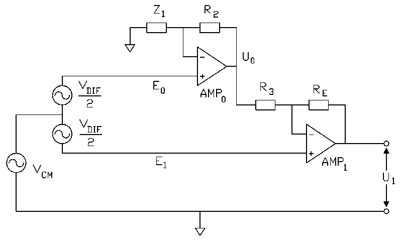
The common mode gain of a two op-amp instrumentation amplifier becomes zero if the
relevant impedances (resistors R2, R3, RE and impedance Z1
in Fig. 1) are chosen according to:
If the condition in Eq. 1 is fulfilled the differential gain of a two op-amp
instrumentation amplifier is given by:
In practice, the CMRR of a two op-amp instrumentation amplifier depends on the matching of
the resistors and the chosen differential gain. A good approximation for the CMRR with
small deviations from the exact resistor ratios is given by:
where: TOLR is the resistor tolerance in %
For example: If the usual 1% tolerance resistors are used for an instrumentation amplifier
with a gain of 1000, a CMRR of 94 dB is achieved without trimming.
The good CMRR of a two op-amp instrumentation amplifier with a high differential gain is a
result of the gain of common mode signals (ACM) being less than unity, even in cases where
the resistor values differ by a large amount from ratios given in Eq. 1. This effect
becomes readily apparent when the gain of the instrumentation amplifier with R2 = 0
(resistor ratios maximally unmatched) is considered for both differential and common mode
input signals (in this case: ACM 1, ADIF is given by Eq. 2 and CMRR = ADIF).
The op-amps in a two op-amp instrumentation amplifier contribute equally to the equivalent
input noise. The two-opamp instrumentation amplifier has good noise properties because an
insignificant contribution of noise sources other than the input op-amps can be achieved
with the gain settings and source impedances found in biomedical recordings. Note that the
noise properties of the two op-amp instrumentation amplifier are equal to the three op-amp
instrumentation amplifier if the latter has sufficient gain in the first amplifier stage.
The two op-amp design seems attractive for the measurement of bioelectric events
because the gain bandwidth product (GBP) of many commercially available low-noise op-amps
is high enough to provide for sufficient differential gain in the bandwidth required. For
example: both EEG (gain 10,000 and a bandwidth of 30 Hz) and ECG (gain 1000 and a
bandwidth of 300 Hz) measurements require a GBP of approx. 300 kHz. Consequently, a single
stage amplifier with one low-noise op-amp providing all gain, would suffice.
The problem of adapting the two op-amp instrumentation amplifier to the biomedical
measurement situation comes down to providing the amplifier with a proper high-pass
response and a sufficient DC input range, without jeopardizing qualities such as high CMRR
and low noise. We achieved this goal with the novel circuit shown in Fig. 2.
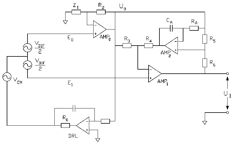
Fig 2 : A novel design for a bio-electric amplifier based on the two opamp instrumentation amplifier. A high pass response is achieved with an intergrator in the feedback loop.
The common mode gain of the modified two op-amp instrumentation amplifier in Fig. 2 is
zero if:
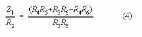
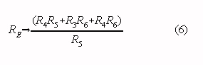
Provided the condition in Eq. 4 is met, the differential gain (ADIF) in the
passband is:
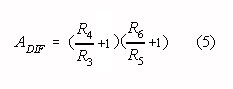
Note that Eqs. 4 and 5 correspond to Eqs. 1 and 2 if the following substitution is made:
The circuit in Fig. 2 is a two op-amp instrumentation amplifier with an integrator in the
feedback loop (AMP2 in Fig. 2). The integrator provides a low overall gain for low
frequency input signals. The high-pass corner frequency is set with RA and CA.
The connection between R5, RA and the output of AMP0 is
essential to attain a high CMRR because it limits the gain for common mode input signals
(ACM) to unity (if R5 and RA were connected to common, the behavior
for differential input signals would be identical, whereas ACM would become very dependent
on exact resistor matching). As a result, Eq. 3 is valid for the modified two op-amp
instrumentation amplifier in Fig. 2 for frequencies above the high pass cut-off frequency
and the good CMRR properties of the basic two op-amp instrumentation amplifier are
retained.
Below the high pass cut-off frequency the common mode gain of the amplifier in Fig 2.
rises by 6 dB/octave to a maximal value of unity. Consequently, for frequencies below the
high-pass cut-off frequency, the CMRR drops from the value given by Eq. 3 to a value equal
to ADIF.
In Fig. 2 a driven right leg (DRL) circuit is used as a connection between the signal
source and the amplifier common (0 V, the midpoint between the supply voltages). A DRL
circuit reduces the common mode voltage by driving U0 (see Fig. 2.) actively to the
potential of the amplifier common (MettingVanRijn et al,. 1990). A DRL, in addition,
protects the patient from the consequences of amplifier defects because a series resistor
in the circuit (R0 in Fig. 2) limits the maximum current through the ground
electrode to a safe level. The common mode suppression of a DRL circuit increases with
decreasing frequency. Consequently, the DRL circuit compensates for the decreasing CMRR of
the instrumentation amplifier in Fig. 2 at low frequencies. In our view, a DRL should be
used in every biomedical recording system for interference suppression and patient safety.
Therefore, when the instrumentation amplifier of Fig. 2 is compared with other designs
with respect to the needed number of parts, the DRL circuit should not be regarded as a
particular complexity of the design in Fig. 2.
Besides the high CMRR, the good noise properties of the basic two op-amp instrumentation
amplifier are retained as well in the modified two op-amp instrumentation amplifier in
Fig. 2. The extra noise generated by AMP2 is divided by the factor R3/(R3+R4)
(approx. 10 - 30 in typical biomedical applications, see also section 4) before it is
added to the input of AMP1. Consequently, the equivalent input noise level of the circuit
is not significantly higher than the combined input noise of op-amps AMP0 and
AMP1.
The low-pass corner frequency of the modified two op-amp instrumentation amplifier depends
on the GBP of op-amp AMP1 and the selected differential gain (the op-amps in
this section are assumed to be internally compensated):
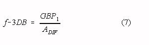
where: GBP1 is the Gain Bandwidth Product of op-amp AMP1 ADIF
is the differential gain of the amplifier The slope of the amplitude characteristic is -6
dB/octave above this frequency. It was established that the differences in GBP between
different op-amps of one type were only a few percent for most popular types.
Consequently, employing the limited GBP of op-amps was found to be a convenient method of
providing the needed low-pass response with sufficient accuracy of the cut-off frequency.
The design is unconditionally stable and no resonances occur with typical compensated
op-amps and the usual gains used in recordings of bioelectric events (see Appendix 2).
The output voltage of op-amp AMP2 in the circuit shown in Fig. 2, is equal
to the DC voltage between the amplifier inputs (E0 and E1)
multiplied by the ratio (R3+R4)/R3. However, since the
output voltage of op-amp AMP2 is limited by the supply voltage, the DC input
range is determined by the resistor ratio (R3+R4)/R3 and
a high value for this ratio reduces the maximum allowable electrode offset. On the other
hand, a low ratio (R3+R4)/R3 allows noise from AMP2
to contribute significantly to the total amplifier noise. Therefore, a trade-off between
DC input range and total noise figure has to be made.
The offset voltage at the amplifier output (U1) of the circuit in Fig. 2 is the input
offset voltage of op-amp AMP2 multiplied by the resistor ratio (R5+R6)/R5.
In cases where a high differential gain ADIF is chosen, the output offset can
become unacceptably high even if AMP2 is of a low offset type. A solution is
the addition of a second integrator as pictured in the practical example in Fig. 3
(integrator around AMP3). The output offset of an amplifier channel (U1 ... UN)
in Fig. 3 is equal to the input offset of op-amp AMP3.
The op-amps used for the integrators in the circuits shown in Figs. 2 and 3 should have
low input bias currents (i.e. JFET, MOSFET or CMOS type op-amps) to allow the selection of
large resistances RA and RB - which is necessary to reduce the size
of the integrator capacitors CA and CB - without producing large
offset voltages between the inputs of op-amps AMP2 and AMP3. Since
the closed-loop gain for noise voltages across the resistors RA and RB
is much smaller than ADIF, thermal noise generated by these resistors as well
as current noise generated by the input bias currents of op-amps AMP2 and AMP3
generally does not add significantly to the total amplifier noise. The design is easily
expanded to more channels, as shown in the example in Fig. 3. Each channel amplifies the
signal between its input (E1 ... EN) and the E0 reference
input (monopolar configuration). Note that the common mode input impedance is equal for
all inputs, an important condition to prevent interference (MettingVanRijn et al., 1990).
A reduction of the bandwidth can be accomplished with a capacitor parallel to resistor R6.
However, appropriate modification of Z1 will then be necessary to retain a high
CMRR. A better method is to reduce the gain-bandwidth-product of op-amp AMP1
since the CMRR does not depend on the bandwidth of this op-amp. Depending on the type of
op-amp, several methods are available. For example: capacitive feedback from the output to
one of the offset pins, selection of a proper compensation capacitor (uncompensated
op-amps) or the selection of a proper set current (programmable op-amps).
An increased bandwidth can be achieved when an uncompensated op-amp is employed for AMP1.
As the ratio of the open-loop gain to the closed-loop gain is small in designs with a high
differential gain, stable operation can be realized with much less compensation than is
provided in a compensated op-amp (Horowitz and Hill, 1989). The application of an
uncompensated op-amp is attractive since the power consumption of such an amplifier at a
given combination of gain and bandwidth is lower than is the case with the application of
a compensated op-amp with a high GBP (see also Appendix 1).
Latch-up may occur if the common mode input range of op-amps AMP2 and AMP3 is smaller than
the output voltage swing of the op-amps AMP0 and AMP1. Therefore, some combinations of
op-amps will require appropriate output clamping of op-amps AMP0 and AMP1.
The output AMP0 may be used to drive guarding and DRL circuits (MettingVanRijn
et al., 1990) as shown in Fig. 3. Adding these circuits will effectively reduce the
susceptibility for power line induced interference: the effective CMRR may be increased up
to 50 dB at 50 Hz and interference currents in the electrode leads are prevented.
In applications with a low differential gain ADIF, the closed-loop response of op-amp AMP0
has a relatively large influence on the CMRR. If Z1 is a resistor, the
decreasing open-loop gain of AMP0 at higher frequencies results in an increasing
closed-loop gain error which in turn will lead to a decreasing CMRR at high frequencies.
For a part, this effect can be counteracted by the use of a capacitor and resistor in
parallel for the impedance Z1 (Z1 = R1/C1). It
can be shown that a good approximation for the optimal value of this capacitor C1
is given by:
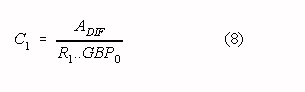
where: GBP0 is the Gain Bandwidth Product of op-amp AMP0
ADIF is the differential gain of the amplifier
On the other hand, in applications with a high differential gain ADIF, the CMRR
is not significantly degraded if Z1 is omitted and R2 is replaced by
a short (see Fig. 3). The selection of specific components for various applications and
the optimization of the amplifier with respect to various specifications, is discussed in
detail in Appendix 1.
An impression of the reduction in number of parts able to be achieved with the design in Fig. 2 is given in Table 1. In this table the circuit in Fig. 2 is compared with a three op-amp design (Neuman, 1978) and with a long tailed pair design (MettingVanRijn, et al, 1991a). All three designs were dimensioned so as to offer a first order bandpass response between 0.16 and 100 Hz with a passband gain of 1000. All designs are one channel differential amplifiers. The circuits are compared without DRL and guard circuits. It follows from table 1 that the three op-amp design and the long tailed pair design require respectively 60 % and 100 % more parts than the design in Fig. 2. It will be clear that with the modern trend to record more and more channels (the use of 32 channels is fairly common in clinical EEG, in experimental settings 64 channel ECG and 128 channel EEG recordings are performed) the savings in cost, dimensions and complexity can be considerable. The design in Fig. 2 is easily modified for other recordings where small differential AC signals are to be measured in the presence of relatively large differential DC signals and high CM signals. The only restriction is that the overall gain chosen must be relatively high - say more than 1000 with typical component tolerances - or the CMRR will be degraded (see Eq. 3).
A new design is presented which greatly simplifies the design of amplifiers for bioelectric events. The design is easily adapted to various biomedical measurement conditions: i.e gain, bandwidth and number of channels are easily changed. The specifications are comparable or better than achievable with the best designs currently available if proper op-amps are chosen (see Appendix 1 and Table 1). The design offers major reductions in size and power consumption compared with conventional designs.
This research was supported by the Technology Foundation (STW).
Cooper, R., Osselton, J. W. and Shaw, J. C. (1969) EEG Technology. Butterworth, London, 14-22.
Geddes L. A. (1972) Electrodes and the measurements of bioelectric events. John Wiley & Sons, New York, 44-94.
Graeme, J. G. (1973) Applications of operational amplifiers: third generations techniques. McGraw-Hill, New York, 53-58.
Graeme, J. G. (1977) Designing with operational amplifiers: application alternatives. McGraw-Hill, New York, 31-35.
Horowitz, P. and Hill, W.(1989) The art of electronics, 2nd edn. Cambridge University Press, Cambridge, 242-248, 425-428.
Huhta, J. C., Webster, J. G. (1973) 60-Hz interference in electro-cardiography. IEEE Trans., BME-20, 91-101.
MettingVanRijn, A. C., Peper, A. and Grimbergen, C. A. (1990) High quality recording of bioelectric events. Part 1: Interference reduction, theory and practice. Med. & Biol. Eng. & Comput., 28, 389-397.
MettingVanRijn, A. C., Peper, A. and Grimbergen, C. A. (1991a) High quality recording of bioelectric evenifiers (op-amps).
APPLICATION EXAMPLE.
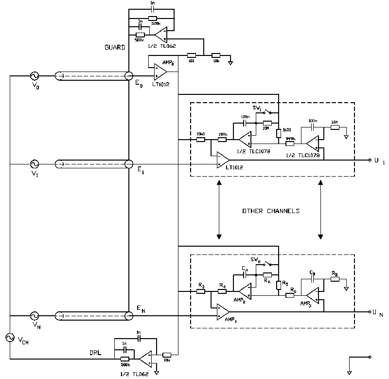
Fig 3. : An example of a multichannel EEG amplifier with minimal noise, a low parts count and a low power consumption. An extra intergrator has been added in the feedback loop to redude the output offset. A DRL and a guard circuit are used for maximal interference reduction.